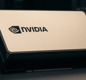
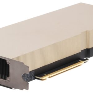
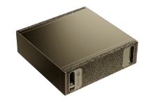
NVIDIA PRO A100 Tensor Core

Description
Designed for AI, HPC, and data analytics workloads:
* NVIDIA A100 GPU (Ampere Architecture) – Key Specifications
* Category * Specification *
*——————– *—————————————————*
* GPU Architecture * Ampere (GA100) *
* Process Node * TSMC 7nm *
* FP32 Cores * 6,912 CUDA Cores *
* Tensor Cores * 432 (3rd Gen) *
* RT Cores * None (Not designed for ray tracing) *
* FP64 Performance * 19.5 TFLOPS *
* FP32 Performance * 19.5 TFLOPS *
* TF32 Performance * 156 TFLOPS (with Tensor Core acceleration) *
* INT8 Performance * 624 TOPS (with Sparsity) *
* Memory (VRAM) * 40GB or 80GB (HBM2e) *
* Memory Bandwidth * 1,555 GB/s (40GB) / 2,039 GB/s (80GB) *
* NVLink Bandwidth * 600 GB/s (3rd Gen NVLink) *
* PCIe Support * PCIe 4.0 x16 *
* TDP (Power) * 250W (40GB) / 400W (80GB) *
* Form Factors * SXM4 (for servers) / PCIe (for workstations) *
* Multi-GPU Scaling * NVLink & NVSwitch for multi-GPU systems (e.g., DGX A100) *
* Key Features * – MIG (Multi-Instance GPU) – Splits GPU into 7 isolated instances <br> – Sparsity Acceleration – 2x speed for sparse AI models <br> – 3rd Gen NVLink – Scalable to multi-GPU systems *
* Use Cases :
✔ AI Training/Inference (GPT-3, recommender systems)
✔ High-Performance Computing (HPC) (scientific simulations)
✔ Data Analytics (big data processing)
✔ Cloud Acceleration (AWS, Azure, Google Cloud instances)
* Performance Highlights
– 5x faster than previous-gen V100 in AI workloads (TF32/FP16).
– Supports MIG for cloud GPU partitioning (e.g., 7x 5GB GPU instances).
– PCIe 4.0 & NVLink for high-speed multi-GPU scalability.
Reviews
There are no reviews yet.